PCB Double Side
PCB Double Side
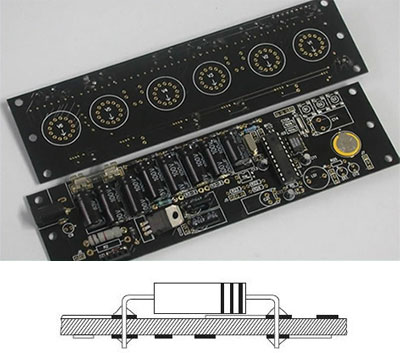
Double-sided printed circuit boards have wiring patterns on both sides of the insulating material, i.e. the circuit pattern is available both on the components side and the solder side. Obviously, the component density and the conductor lines are higher than the single-sided boards.
- Double-sided board with plated through-hole connection (PTH)
- Double-sided board without plated through-hole connection (non-PTH)
Double-sided PTH board has circuitry on both sides of an insulating substrate, which is connected by metallizing the wall of a hole in the substrate that intersects the circuitry on both sides. This technology, which is the basis for most printed circuits produced, is becoming popular in cases where the circuit complexity and density is high.
Double-sided non-PTH board is only an extension of a single-sided board. Its cost is considerably lower because plating can be avoided. In this case, through contacts are made by soldering the component leads on both sides of the board, wherever required. In the layout design of such boards, the number of solder joints on the component side should be kept to a minimum to facilitate component removal, if required. It is generally recommended that conductors should be realized as much as possible on the non-component side and only the remaining should be placed on the component side.